New research could enable an explosion of very inexpensive, very high resolution 3D scanners.
3D scanning is a technology tightly related to 3D printing: it’s one of the key approaches for generating 3D models for printing. To obtain a 3D scan, however, it’s a lot trickier than one might think.
There are only a few methods of 3D scanning widely used these days:
- Laser ranging, where a laser traces over an area and measures the bounce-back time to determine the distance to each pixel of the image
- Infrared capture, where a coarse array of infrared beams covers a small area, and the bounce-back times are measured to determine distance
- Structured light, where a standard light pattern is projected onto a surface and the distortions are analyzed as it moves across the object
- Photogrammetry, where a (large) collection of images taken of an object from all angles is analyzed to determine the 3D geometry
All of these methods work reasonably well, but they do have constraints of one type or another. Photogrammetry, for example, requires a ton of images and even more tons of processing afterwards. Light-based techniques only offer a small “active” zone for capture and provide relatively coarse results.
But now there may be a new approach that could invalidate all of these methods.
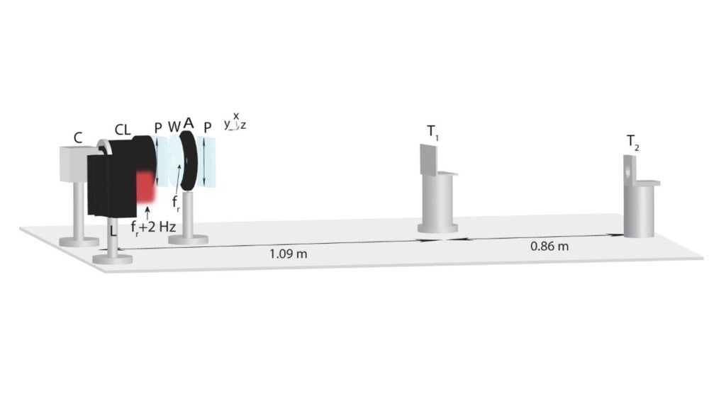
In a paper entitled, “Longitudinal piezoelectric resonant photoelastic modulator for efficient intensity modulation at megahertz frequencies”, researchers have found a way to modify a standard CMOS light sensor (the same type found in smartphones) to capture depth information similar to the light-based approaches above.
How does this work? It’s actually quite ingenious.
A normal CMOS image sensor simply captures an array of pixels, with color and light intensity information for each. These have been made more dense over the years, and now it’s possible to obtain huge sensors with dozens of megapixels for each capture.
But there’s no depth information for those pixels.
The idea is to place another light source beside the image sensor, which blasts out a varying and predictable range of light frequencies. Imagine this light source changing its frequency millions of times per second, far, far faster than the regular image capture elapsed time.
Because of the rapidly changing frequencies, the light captured by the image sensor will have different frequencies detected on each pixel because the other light source will have changed. That’s because the different bounce-back distances have sufficient time for the secondary light source to change frequency.
In other words, each pixel should have depth information, discernible by appropriate software. The regular image sensor is now a 3D depth sensor!
The key to this technology is the modulator, which can change the frequencies at a stupendous rate. The researchers found that lithium niobate, a piezoelectric material, can do just that on a very reliable basis. By coupling this modulator with polarizing filters, the light can be altered.
This is an amazing development, and it has multiple implications.
First, 3D scanners could be made with massively higher resolutions. It would also be possible to capture scans far more quickly due to the huge sensor sizes on current CMOS chips. However, the added data collected would also likely require similar increases in processing power.
Another implication is that the cost of 3D scanners could drop significantly. It might be possible, for example, to include one of these modulators in a smartphone — meaning everyone might be carrying around a super-scanner in their pocket in coming years. It could then become routine to capture highly detailed 3D scans on a whim.
Via Nature

