
The Freeform Multi-material Assembly Process from the University of Missouri enables the production of complex devices with materials including plastics, metals, and semiconductors.
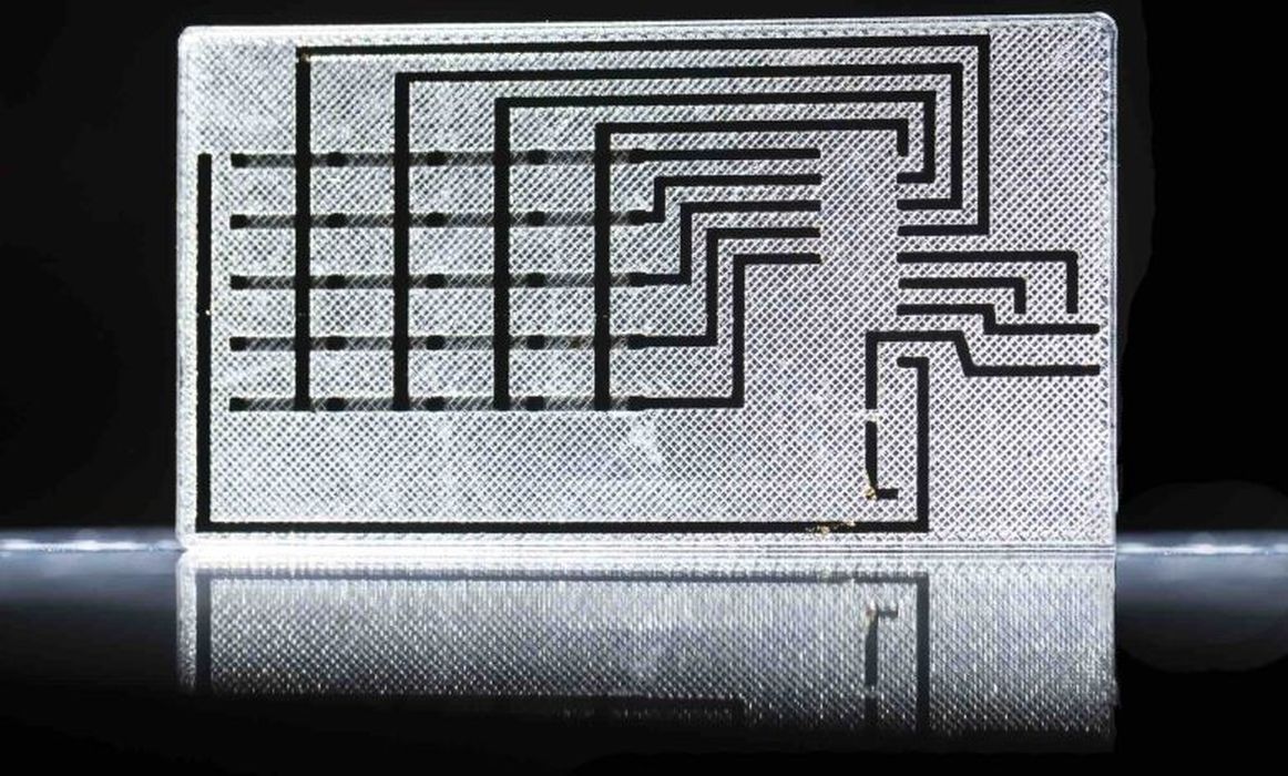
According to the University of Missouri, researchers have developed a way to create complex devices with multiple materials – including plastics, metals, and semiconductors – all with a single machine. The research, which was recently published in Nature Communications, outlines a novel 3D printing and laser process – called the Freeform Multi-material Assembly Process – to manufacture multi-material, multi-layered sensors, circuit boards, and even textiles, with electronic components.
By printing sensors embedded within a structure, the machine can make objects that can sense environmental conditions, including temperature and pressure. For other researchers, this could mean having a natural-looking object such as a rock or seashell that could measure the movement of ocean water. For the public, applications could include wearable devices that monitor blood pressure and other vital signs.
“This is the first time this type of process has been used, and it’s unlocking new possibilities,” said Bujingda Zheng, a doctoral student in mechanical engineering at the University of Missouri and the lead author of the study. “I’m excited about the design. I’ve always wanted to do something that no one has ever done before, and I’m getting to do that here at Mizzou.”
One of the main benefits is that innovators can focus on designing new products without worrying about how to prototype them. “This opens the possibility for entirely new markets,” said Jian Javen Lin, an associate professor of mechanical and aerospace engineering at the University of Missouri. “It will have broad impacts on wearable sensors, customizable robots, medical devices, and more.”
Currently, manufacturing a multi-layered structure – such as a printed circuit board – can be a cumbersome process that involves multiple steps and materials. These processes are costly, time-consuming, and can generate waste that harms the environment.
“Everything in nature consists of structural and functional materials,” said Zheng. “For example, electrical eels have bones and muscles that enable them to move. They also have specialized cells that can discharge up to 500 volts to deter predators. These biological observations have inspired researchers to develop new methods for fabricating 3D structures with multi-functional applications, but other emerging methods have limitations.”
Specifically, other techniques fall short when it comes to how versatile the material can be and how precisely smaller components can be placed inside larger 3D structures.
Read the rest of this story at VoxelMatters