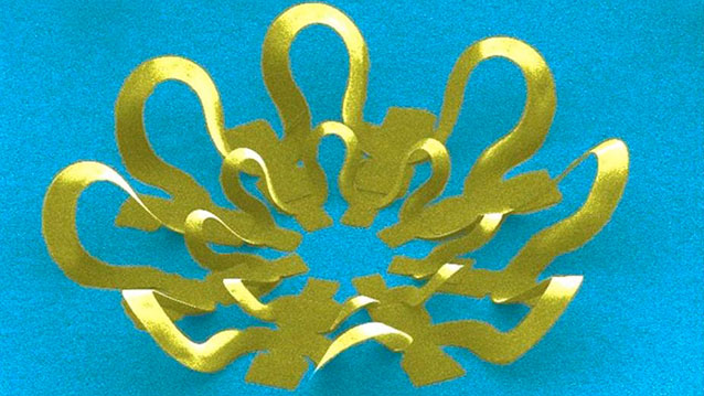
Researchers at Northwestern University and the University of Illinois at Urbana-Champaign have developed a simple new fabrication technique to create beautiful and complex 3-D micro- and nanostructures with many advantages over 3-D printing.
The technique mimics the action of a children’s pop-up book — starting as a flat two-dimensional structure and popping up into a more complex 3-D structure. Using a variety of advanced materials, including silicon, the researchers produced more than 40 different geometric designs, including shapes resembling a peacock, flower, starburst, table, basket, tent and starfish.
“In just one shot you get your structure,” said Northwestern’s Yonggang Huang, one of three co-corresponding authors on the study. “We first fabricate a two-dimensional structure on a stretched elastic material. Then we release the tension, and up pops a 3-D structure. The 2-D structure must have some place to go, so it pops up.”
The pop-up assembly technique trumps 3-D printing on many levels and is expected to be useful in building biomedical devices, sensors and electronics.
Details of the technique, which relies on compression buckling, will be published as the cover story Jan. 9 in the journal Science.
The study is a demonstration of a new and innovative approach to creating 3-D structures, Huang said. Determining which designs are needed for specific applications will come in future research.
Huang led the portion of the research focused on theory, design and modeling. He is the Joseph Cummings Professor of Civil and Environmental Engineering and a professor of mechanical engineering at Northwestern’s McCormick School of Engineering and Applied Science.
The advantages of the new pop-up method are numerous. The technique is fast and inexpensive, and it can: be used to build many different structures at one time; utilize many different materials, including silicon; incorporate different materials into one hybrid structure; be used to build structures on both micro- and nano-levels (down to a thickness of 100 nanometers); and produce a wide range of different geometries.
Read more at ENGINEERING.com

